
Prelim: What is FPGA?
Introduction
Putting CPU and FPGA together has been an old idea that dates back to the beginning of the 21st century. This article reflects on my ideas after reading several relevant papers.
Here is the list of papers involved:
- Garp: T. J. Callahan, J. R. Hauser and J. Wawrzynek, "The Garp architecture and C compiler," in Computer, vol. 33, no. 4, pp. 62-69, April 2000, doi: 10.1109/2.839323.
- PRISC: R. Razdan and M. D. Smith, "A high-performance microarchitecture with hardware-programmable functional units," Proceedings of MICRO-27. The 27th Annual IEEE/ACM International Symposium on Microarchitecture, San Jose, CA, USA, 1994, pp. 172-180, doi: 10.1145/192724.192749.
- PipeRench: H. Schmit, D. Whelihan, A. Tsai, M. Moe, B. Levine and R. Reed Taylor, "PipeRench: A virtualized programmable datapath in 0.18 micron technology," Proceedings of the IEEE 2002 Custom Integrated Circuits Conference (Cat. No.02CH37285), Orlando, FL, USA, 2002, pp. 63-66, doi: 10.1109/CICC.2002.1012767.
- Chimera: S. Hauck, T. W. Fry, M. M. Hosler and J. P. Kao, "The Chimaera reconfigurable functional unit," in IEEE Transactions on Very Large Scale Integration (VLSI) Systems, vol. 12, no. 2, pp. 206-217, Feb. 2004, doi: 10.1109/TVLSI.2003.821545.
CPU-FPGA Interconnect/Communication
FPGAs in such settings are often used as a reprogrammable accelerator that accompanies the CPU. There are multiple communication models between the CPU and the FPGA, which can be divided into two big categories: tightly coupled or loosely coupled.
Loosely coupled means that the CPU communicates with the FPGA through some interconnect. Examples include connecting the FPGA to the CPU's L1, L2 or Last-level cache. The FPGA may also connect to the CPU's On-Chip Network (NoC) or other types of internal interconnect. To bring the distance further away, the FPGA can also connect to the CPU with external buses, such as PCIe. In these cases, the CPU explicitly issue commands to the FPGA through memory-mapped IO, and data transfer is copy-in/copy-out.
Tightly coupled refers to a design where an FPGA is highly integrated with the CPU, essentially becoming a functional unit for the CPU. In such designs, the reprogrammable logic may be part of the CPU's pipeline or connected to the register file of the CPU. Instead of visiting the reprogrammable logic with explicit data transfer instructions, the FPGA may change how CPUs interpret instructions or add new instructions that the CPU can execute by utilizing the FPGA part.
Loosely coupled architectures are more popular and more widely used for accelerators nowadays. GPUs, for example, connect to the CPU with PCIe. Such systems are easy to design and cheap to implement. It is easy to add them to existing systems. Tightly coupled systems, on the other hand, are less researched. Such systems require designing new chips. Clock management also becomes a problem since FPGAs are much slower than dedicated functional units. Putting them into the processor's datapath may introduce long critical paths that force the processor to slow down its clock.
Designs
Garp
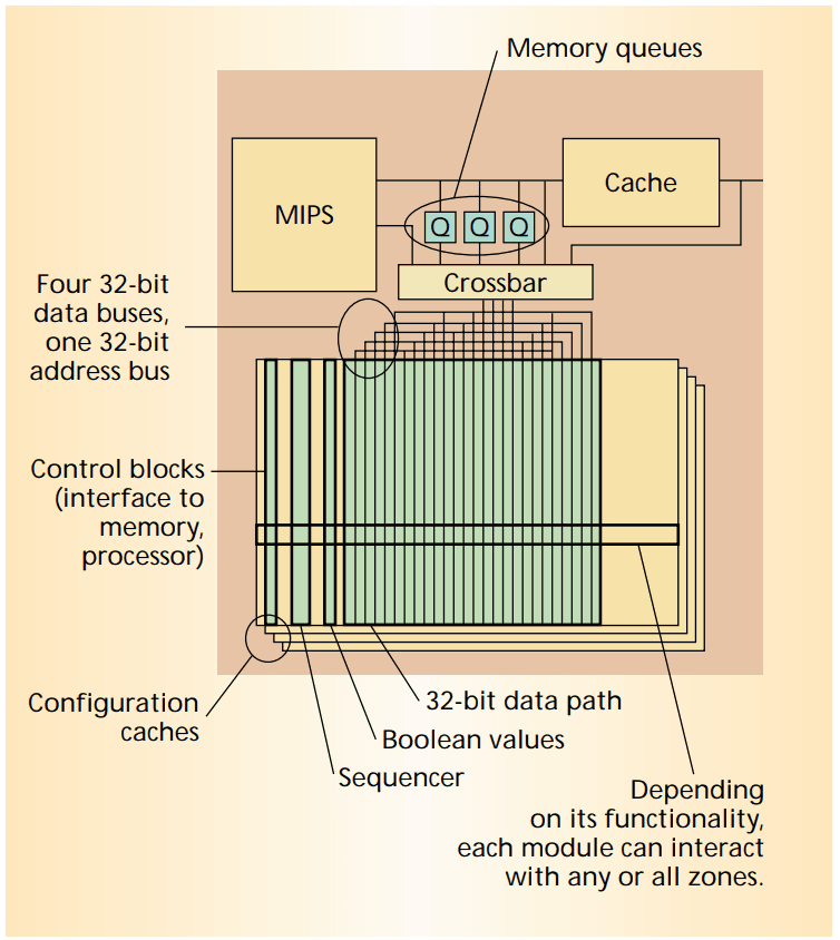
The Garp architecture contains a reprogrammable logic array, connected to the CPU with a memory bus. The CPU transmits data to the Garp array just like accessing the memory. The reprogrammable array is equipped with four configuration caches, so it may quickly switch between four different configurations.
The Garp array can also access the memory by programming one row to supply the read address, and the data will feed into another row after a fixed number of clock cycles. The memory delay is explicitly specified in the configuration; if the memory is not able to respond that fast, the whole array is stalled.
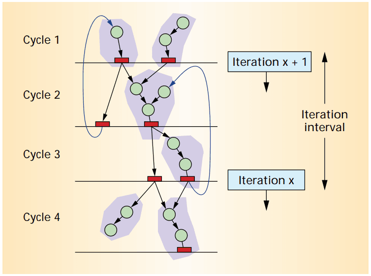
This paper focused less on how Garp is internally designed and implemented but more on what it can achieve. In the author's vision, programs can be abstracted as a dataflow, and the dataflow diagram can be mapped to the FPGA, as shown above. Multiple steps in the DFG can be combined and overlapped thanks to the width of the FPGA, and the whole DFG can be pipelined to achieve higher clock speeds and additional parallelism.
This makes the Garp design essentially a VLIW processor: Each stage performs multiple operations at the same time. However, it is not limited by the fixed function units of a VLIW processor: Each stage has its hardware programmed to do precisely what is needed.
The efficiency of Garp is simulated with a cycle-accurate simulator, and it outperforms pure CPU designs by a large margin on image and vector workloads.
PRISC
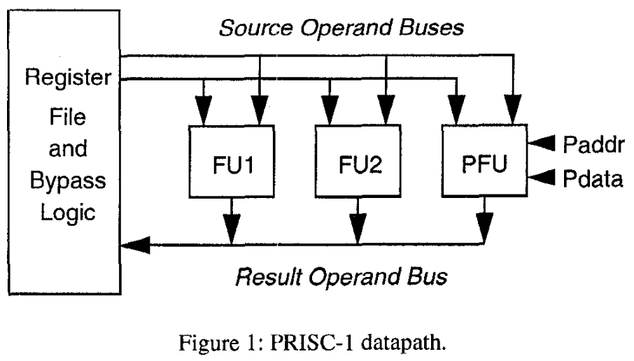
PRSIC here means "PRogrammable Instruction Set Computers." As the name suggests, it is a tightly integrated architecture that uses FPGA as a programmable function unit. The function unit occupies the same position as fixed function ALU datapaths.
FPGAs are inherently much slower than dedicated ASIC logic if they were to implement the same functionality. Therefore, the programmable function unit is an augmentation of the usual function units rather than completely replacing them. The programmable function unit can only accept two operands and output one result, like any other functional unit. This limits what the PFU can do. In the evaluation part, the PFU is mostly used to optimize sequential logic or arithmetic operations, combining multiple instructions into one.
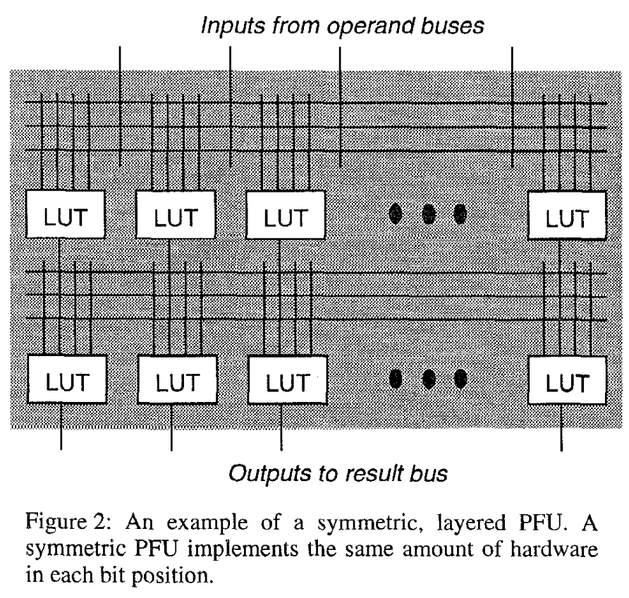
The design of PFU is shown above: stacked, alternating layers of interconnects and LUTs. The operands come from above, and the results appear below. The output of each LUT is only fed to the next layer, and they may not communicate within the same layer. To cut the critical path short and fit in the cycle of microprocessors back then, the authors chose a 3-layer PFU that should fit into 200MHz microprocessors.
The author also talked extensively about compiling and optimizing the code.
Chimaera
Chimaera, similar to PRISC, is also a tightly-integrated design with a programmable function unit. However, it tries to make the reprogrammable logic more specifically designed for being integrated into the CPU, and it tries to solve the restriction of two operands.
The reconfigurable array is seen as a purely combinational logic with no clock. A shadow register file is included, copying a subset of the host register file so that the reconfigurable array can access at most 9 registers as operands. Since this reconfigurable array is purely combinational, there isn't an instruction to send operands to it. There is an instruction to retrieve the result from the configurable array. Therefore, the whole workflow work as follows: The processor prepares the operands and puts them into registers. Then it decides whether it wants to wait a couple of cycles and let signals propagate through the array. Finally, it uses the instruction RFUOP to retrieve the result and save it to a register.
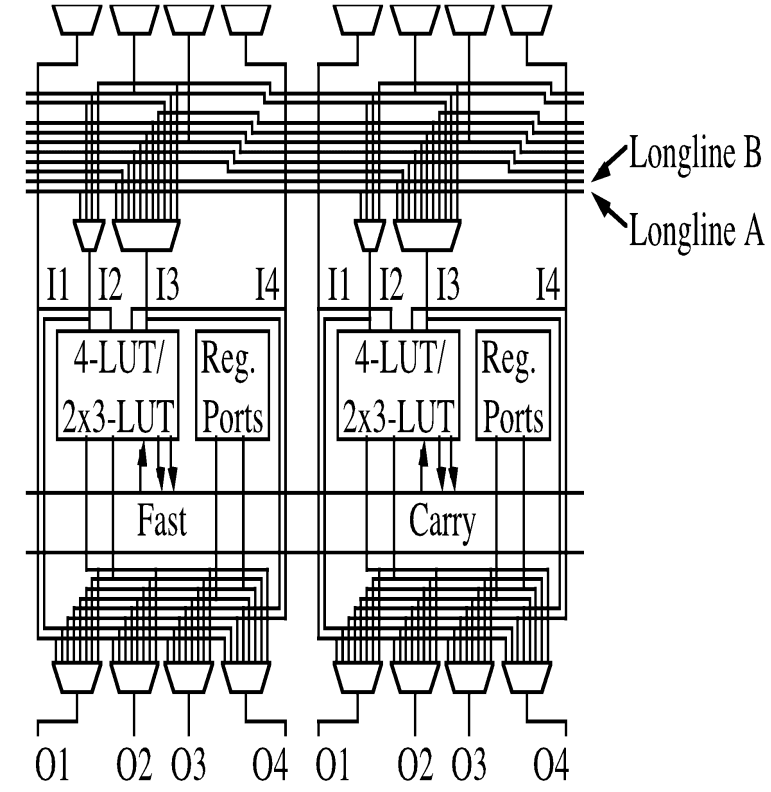
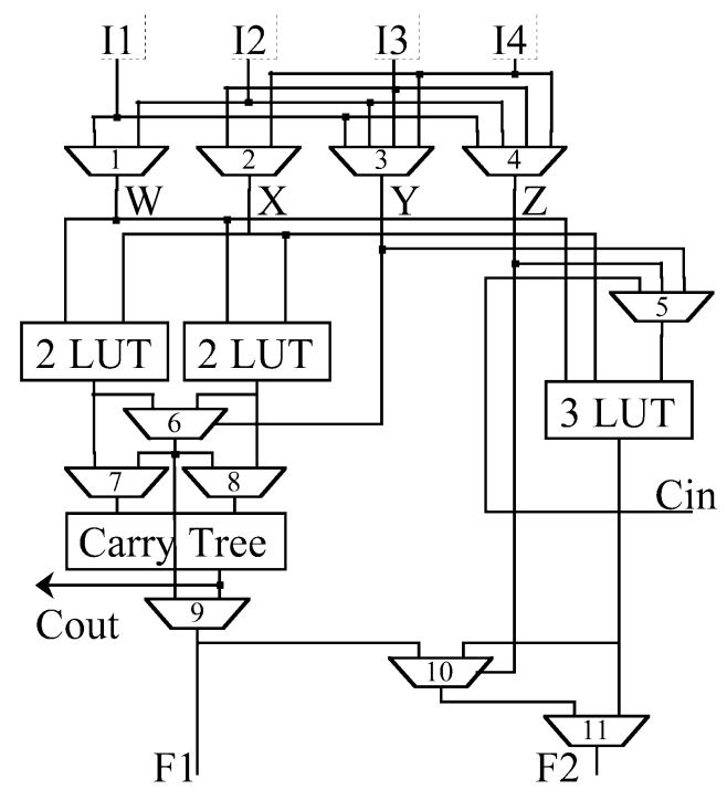
Shown to the left are two cells of the reprogrammable array. For 32-bit processors, there will be 32 such cells in a row. Shown to the right is the detailed design of the "4-LUT/2x3-LUT" block on the left. The logic design is very, very unconventional and weird. As the authors claimed, this structure was created by analyzing several candidate code segments and extracting logic structures that would be the most beneficial.
Like Garp, Chimaera also has configuration caches, allowing fast reprogramming.
PipeRench
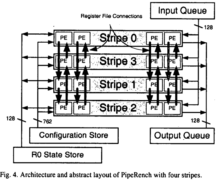
PipeRench is not a complete CPU, just a datapath. It is something you may see in a DSP. Data is fed in and out with FIFO queues.
In the PipeRench architecture, the datapath consists of several stripes, and each stripe consists of 16 processing elements (PEs). The PEs in each stripe is connected circularly, as shown above. This circular interconnect allowed the implementation of an infinitely-long pipelined datapath: As data flows through each stripe, the other stripes can be reprogrammed on the fly. For example, when data is in stripe 0, a new configuration can be loaded into stripe 1.
The authors used the term "virtual stripes" and "physical tripes": If the amount of virtual stripes is less or equal to the number of physical stripes available, then the datapath only need to be programmed once, and data can be pipelined in and out, achieving some parallelism. If the number of physical stripes is less, then the datapath must be reprogrammed on-the-fly.
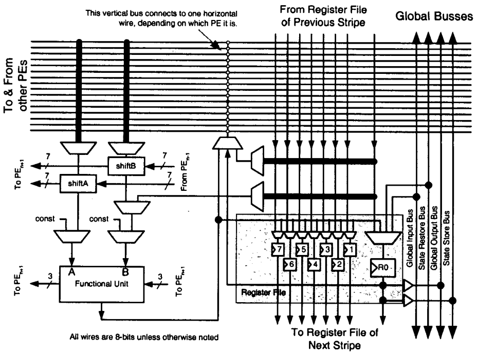
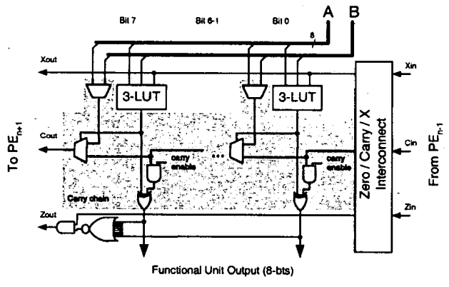
Each processing element contains a register file, some MUX logic for selecting operands, and a function unit that can be programmed to perform some logic.
Conclusion
We saw some quite interesting designs of CPU-FPGA hybrid architectures with different levels of integration and different target applications. These designs came from the beginning of the 21st century when lithography was still on a micron scale, and FPGAs were relatively underdeveloped.
From today's point of view, accelerators are increasingly widespread. Companies like Apple put a lot of different accelerators into their chip design, but some people may never actually utilize some of those accelerators. Approaching the end of Moore's law, it becomes increasingly critical that transistors are utilized effectively. CPU-FPGA hybrid architectures provided a way. Applications can schedule their accelerators to be deployed when they need them and released when they are finished.
This vision would not be that easy. FPGAs, due to their rich programmability, are a poor use of transistors compared to specifically designed ASICs. This program may be solved by Coarse-Grained Reprommable Arrays (CGRAs,) which are less reconfigurable than an FPGA but can operate faster due to more logic paths being hardwired.
With the development of FPGA technologies and other types of reconfigurable hardware, CPU-FPGA hybrid architectures is a promising area for further research.
Comments NOTHING