
Intel Single-Chip Cloud, abbreviated as SCC, is a project that aims to build a cloud-like data center on a single chip. It never really took off, with its last whitepaper released in the year 2010 under a revision number of 0.7, which hints at its beta status.
The result is a manycore processor that bears somewhat traditional 2D-mesh interconnect but with interesting takes on communication and cache coherence.
TL;DR: Main Design Features
- Manycore: A lot of cores on a single chip.
- Not cache-coherent. Core exchange messages through message-passing, just like using ethernet, but on the chip.
Cores and Tiles
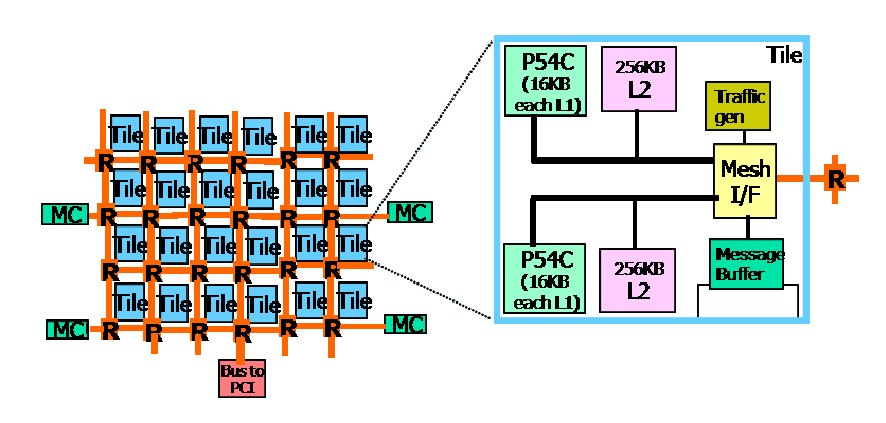
The tiles are laid out in a 2x6 mesh, and each tile contains 2 cores. The cores are Pentium P54C, which is a weird choice since the P54C microarchitecture came out in 1994, discontinued around 2000, yet the SCC was developed in 2009.
Each core has its own 16KB L1 cache and 256KB L2 cache. Both cores are then connected to a mesh interface unit (MIU), which connects to the on-chip network. The MIU handles data packaging and unpackaging, as well as hosting a smaller buffer that queues incoming and outgoing packets.
When both cores want to transmit data, MIU accepts data from the two cores in a round-robin fashion.
On-Chip Network
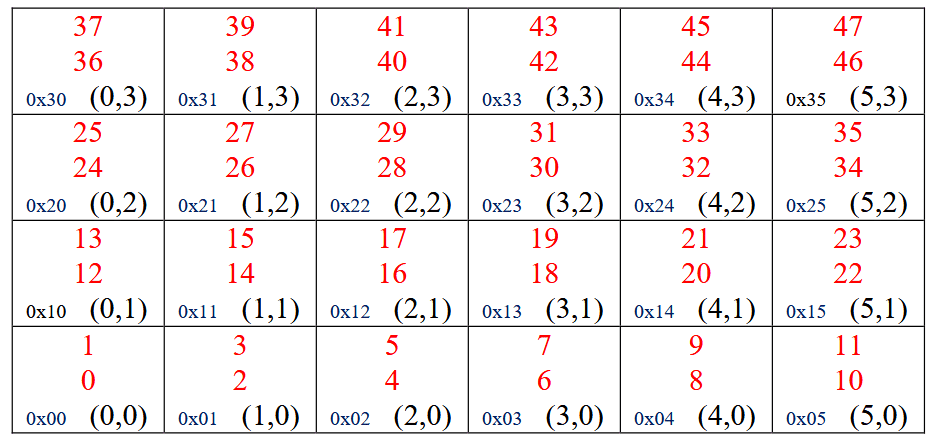
Tiles are indexed with their X and Y coordinates in the mesh, shown above. Each tile has sub-indexes for indexing a core, its message buffer, or peripherals connected to it, as we will see later in Address Translation.
The Mesh Interface Unit (MIU) in each tile has a 16KB message buffer. This buffer is shared across all tiles on the chip, yielding 384KB in total. This 384KB of storage can be directly accessed by each core, but more often it is used through a message-passing interface.
The mesh interface also contained a traffic generator used for testing the performance of the mesh and is not used in normal operations.
The NoC connects to four DRAM memory controllers and a PCIe system interface. Each DRAM memory controller is connected to 16GB of memory, and the PCIe interface is connected to an FPGA on the development board to handle all I/O.
Power and Thermal Management
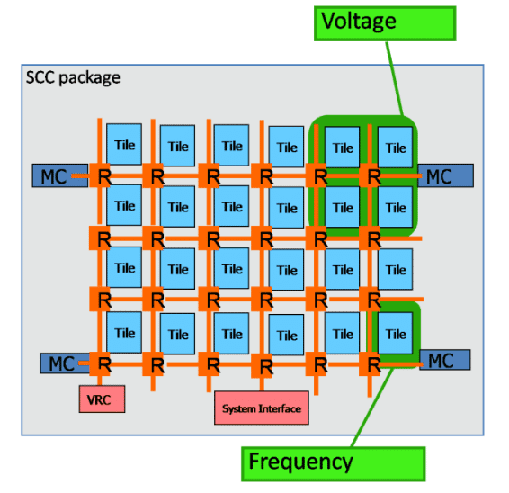
The chip has a single Voltage Regulator Controller (VRC) attached to the tile (x=0, y=0). It can be accessed by all the cores through the NoC. Programs can change the voltage and frequencies for all members of a voltage domain, which is not necessarily the voltage/frequency domain that the program is running in.
Each 4 (2x2) tiles are organized into a voltage domain; each tile has its own frequency domain. The entire set of tiles has an additional voltage domain. Therefore, the chip has 7 voltage domains and 24 frequency domains.
Each tile also has a digital temperature sensor. Its readings are written into a configuration register and allow dynamic scaling of voltage and frequency.
Memory Hierarchy
Each core has a 32-bit memory address space that covers 4GB of memory space, called the core address. The entire system uses system address, which is 46 bits and addresses all components in the system. Address translation happens in the mesh interface unit (MIU), which contains lookup tables (LUTs) to translate core address to system address. There is one LUT for each core.
A core address may get translated into three types of actions. Each action has a queue in the MIU to be executed.
- Memory access: The request will be sent to the router, then to the DRAM controllers, then to the external DRAM memory.
- Message Passing: The request will be sent to the Message Passing Buffer (MPB), either local or remote.
- MIU Local Configuration Registers, which will be handled by the MIU.
Memory Organization
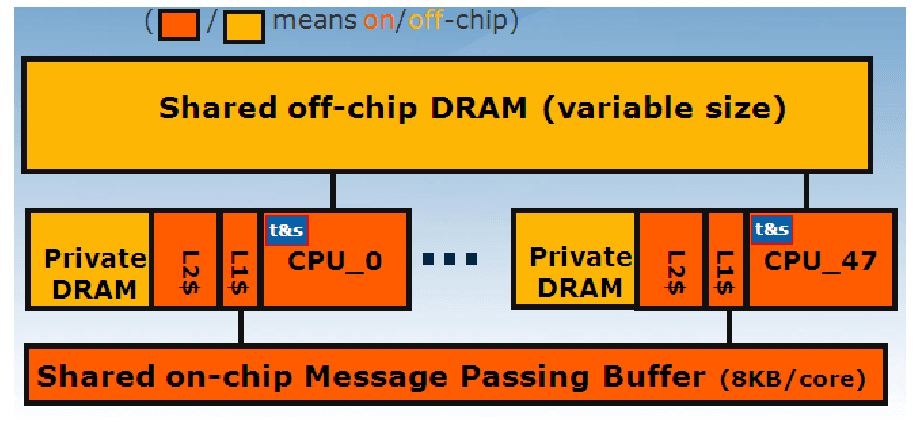
The off-chip DRAM is divided into two portions: Private memory for each core and shared memory among all cores. The amount of private and shared memory is configured through the lookup table (LUT). The default setting is to give each core as much private memory as possible and use the remaining as shared.
This division also affects the routing to DRAM controllers: For private memory access, the request is sent to the specific memory controller assigned for the tile. Shared memory accesses can go through any of the memory controllers.
Address Translation
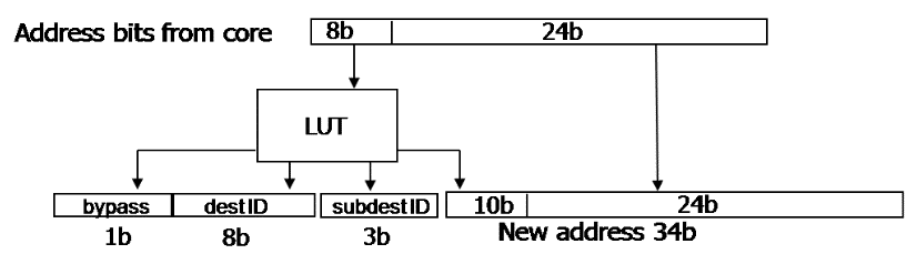
The diagram above shows how the core address is translated to the system address. The lower 24 bits are passed through, and the higher 8 bits are sent into the lookup table.
The lookup table generates three fields: bypass, destID, subdestID, and a 10-bit prefix. They are used as follows:
- bypass: If this bit is 1, then this address refers to the local message passing buffer. destID is ignored.
- destID: Identifies a tile in (y, x) format. For example, tile (y=2, x=5) is encoded as 0010 0101.
- subdestID: Refers to the specific element in the destID tile. It could be one of Core0, Core1, Configuration Registers (CRB), or Message Passing Buffer (MPB). For some specific tiles connected to memory controllers, PCIe system interface, or VRC, it can also choose one of these components using a direction (East, South, West, or North).
- The 10-bit prefix is concatenated with the 24-bit passthrough address to get a 34-bit address, which can be used to address 16GB of memory. There are four memory controllers, and this request will be sent to one specific memory controller, so the total useable memory is 64GB.
Caching
The L1 and L2 cache for each core cache private memory as usual, but the programmer is responsible for explicitly managing cache coherence for shared memory, as this chip was not designed to have any cache coherence.
RCCE is a message-passing programming model from Intel provided with SCC, and it has primitives similar to MPI. If the programmer uses RCCE for communication, then cache coherence is handled by the library automatically. The system provides s special MPBT (Message Passing Buffer Tag) tag that identifies a cache line as shared and an instruction (CL1INVMB) to mark all MPBT lines as invalid.
Some memory latency numbers are given as follows. This is obviously not fast:
- Reading from L2 takes around 18 cycles.
- Reading from local MBP takes around 15 cycles if the bypass bit is set
- Reading from local MBP takes 45 core cycles + 8 mesh cycles if the bypass bit is not set.
- Reading from a remote MBP takes 45 cores cycles + 8*n cycles, where n is the number of hops.
- DDR memory access takes 40 core cycles + 8*2*n mesh cycles to the memory controller, plus 30 cycles at 400MHz memory controller latency and 16 cycles at 400MHz, the DDR frequency.
RCCE
RCCE is pronounced "rocky," and they never mentioned its full name in the document. It is the programming model provided for SCC and has a couple of main functionalities:
- Memory management, such as malloc and free.
- MPI-like interfaces to send and receive messages, including synchronization barriers.
- Power and frequency management.
System Architecture
The system connects to an FPGA through the PCIe system interface, and the FPGA is connected to some peripherals as well as a normal PC through another PCIe interface. The normal PC will be called the Management Console, with drivers and software kits that are designed to work with the SCC. The principle is that an operating system will be loaded onto the cores, and applications will be loaded and run on the OS. I/O system calls are redirected to and handled by the FPGA. All interactions with the system happen through the management console.
This is obviously a lab setup, but given that the project almost never walked out of Intel's research lab, such a setup does match what we are using to test newly developed chips.
Conclusion and Final Thoughts
The Single-Chip Cloud is an interesting take on manycore design. The intention of this project was obvious - to consolidate a data center into a single chip. Each core looks like a computer on the rack, and the on-chip network ties them together just like we connect machines together in a data center. However, the limited amount of memory and outdated-ish cores will not support a lot of cloud applications, not to mention security issues - there was basically no isolation between workloads running on different cores.
This project was brought to my attention because cloud and microservices are being mentioned more and more nowadays. As a result, an application consists of not a single program but a bunch of programs in their own processes, exchanging information between them using networking primitives. They are being deployed as containers, and in the ideal case, one process will be handled by only one core, maximizing the utilization of microarchitectural boosts such as TLBs, cache, and branch prediction. These processes may run better with a couple more threads but do not scale to lots of threads and has little need for shared memory or cache coherency.
As a result, the SCC architecture deployed in the old days happened to meet the needs of new applications. Recent works targeting improving the efficiency of microservices, such as , referred to SCC as a possible yet suboptimal architecture for microservices, pointing out that some cache coherence can help with multi-threaded services.
Wikipedia says this chip is still being actively used for research purposes, but I doubt that new research projects will use platforms that is more open, such as OpenPiton.
Comments NOTHING